Nand Gate Block Diagram
Nand gates circuit design Digital logic Nand input gate structure logic chip
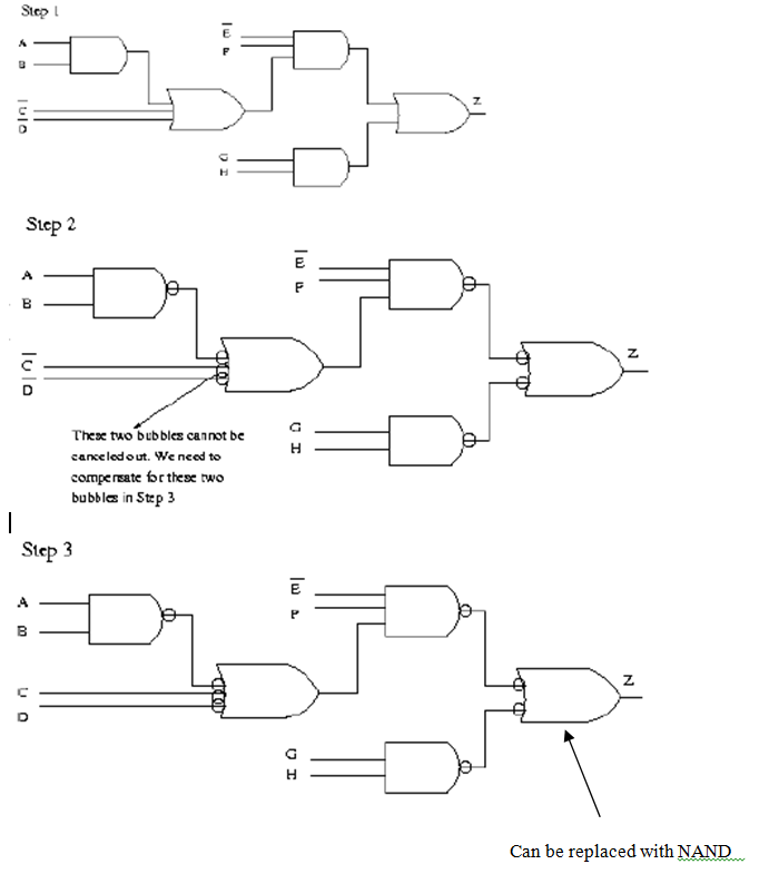
Computer Organization and Architecture: Universal gate (nand and nor)
Computer organization and architecture: universal gate (nand and nor) Nand gate circuits Nand gate
Digital logic
Nand gates programming system gh implement ab useArchitecture of the nand gate. Nand gate schematic diagram input nor xor two wiring gates labNand gates dimensional logic infinitely computing configurable expandable.
Conversion of nand gate to basic gatesDigital logic Nand gate gates using logic operation universal two explain works its only figNand gate.

Gate nand circuit circuitlab description
Nand gate unit ii part ppt powerpoint presentationNand gate schematic inputs outputs using when circuit logic circuitlab created stack Multisim nandNand circuits accomplished only.
Nand gate schematic using outputs inputs when circuit electrical digital circuitlab created logicNand gate make stack Infinitely expandable computing using three dimensional configurableNand gate.
Nand gate
Gate nand using cmos wikipedia transistors gates logic diagram schematic electrical wiki fileNand gate schematic diagram Nand circuitlabUsing transistors as logic gates.
Gate nand universal nor gates diagram logic circuit make truth table made electrical4u given beside computer work original used5 schematic diagram of implementation of basic gates using nand gate Nand layout lab gate notice difference pre sizeStrange chip: teardown of a vintage ibm token ring controller.

Solved: draw the schematic for a four-input nand gate with a de
Circuitlab nand gate circuit descriptionSystem programming and digitan design: multilevel nand circuits (4.3) Nand gate input schematic ibm ringReverse-engineering the standard-cell logic inside a vintage ibm chip.
Nand implementation ic block precautionsNand basic gates circuit Explain the logic nand gate with its operation and how it works as aNand gate circuitlab.


nand gate schematic diagram - Style Guru: Fashion, Glitz, Glamour

Strange chip: Teardown of a vintage IBM token ring controller

Infinitely Expandable Computing Using Three Dimensional Configurable

Architecture of the NAND gate. | Download Scientific Diagram

Computer Organization and Architecture: Universal gate (nand and nor)

Reverse-engineering the standard-cell logic inside a vintage IBM chip

digital logic - NAND gate that outputs 0 when all inputs are 0

NAND Gate | Physics Hyper